.
Keeping this in view, what is enhancement and depletion type Mosfet?
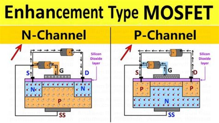
The main difference this time is that MOSFETs are available in two basic forms: Depletion Type – the transistor requires the Gate-Source voltage, ( VGS ) to switch the device “OFF”. Enhancement Type – the transistor requires a Gate-Source voltage, ( VGS ) to switch the device “ON”.
Also Know, what are the types of Mosfet? MOSFETs are available in two basic forms:
- Depletion Type: The transistor requires the Gate-Source voltage (VGS) to switch the device “OFF”. The depletion mode MOSFET is equivalent to a “Normally Closed” switch.
- Enhancement Type: The transistor requires a Gate-Source voltage(VGS) to switch the device “ON”.
Keeping this in view, why is Enhancement type Mosfet preferred?
Actually enhancement MOS is preferred over depletion MOS, mainly bcz EMOS is easier to fabricate as compared to DMOS. Also on EMOS, channel is formed due to gate voltage while in DMOS, channel is pre fabricated.
What is difference between enhancement and depletion mode?
Enhancement mode devices require a voltage to be applied to turn them on (make them conduct). The voltage enhances the devices by forming a channel that conducts. Depletion mode devices normally conduct and a voltage is applied to turn them off (make them stop conducting).
Related Question AnswersWhat is meant by depletion mode?
depletion mode. A transistor that is normally closed (on), allowing current to pass, but is triggered to open (off) and impede current. Contrast with "enhancement mode," wherein the transistor is normally open (off), but is triggered to close (on). THIS DEFINITION IS FOR PERSONAL USE ONLY.What do you mean by CMOS?
1. Alternatively referred to as a RTC (real-time clock), NVRAM (non-volatile RAM) or CMOS RAM, CMOS is short for complementary metal-oxide semiconductor. CMOS is an onboard, battery powered semiconductor chip inside computers that stores information.What is meant by enhancement mode?
Enhancement-mode MOSFETs (metal–oxide–semiconductor FETs) are the common switching elements in most integrated circuits. These devices are off at zero gate–source voltage. In most circuits, this means pulling an enhancement-mode MOSFET's gate voltage towards its drain voltage turns it ON.What is pinch off voltage?
Pinch off voltage: Pinch off voltage is the drain to source voltage after which the drain to source current becomes almost constant and JFET enters into saturation region and is defined only when gate to source voltage is zero.What is eMOSFET?
Enhancement MOSFET, or eMOSFET, can be classed as normally-off (non-conducting) devices, that is they only conduct when a suitable gate-to-source positive voltage is applied, unlike Depletion type mosfets which are normally-on devices conducting when the gate voltage is zero.Why Mosfet is a voltage controlled device?
The MOSFET, like the FET, is a voltage controlled device. A voltage input to the gate controls the flow of current from source to drain. The gate does not draw a continuous current. Though, the gate draws a surge of current to charge the gate capacitance.Why SiO2 is used in Mosfet?
1.1 MOSFET SiO2 is used to avoid direct charge flow from the gate to the channel and vice-versa. SiO2 layer is used as an electrical isolation between the gate and the channel through which major conduction will take place. SiO2 is used as base insulating layer on which the other layers (Drain, Source, etc.) are grown.At what voltage does a Mosfet turn on?
If you want to fully turn on the MOSFET as a switch then the voltage needs to be significantly higher than Vgs(th). Look in the transistor specification table for the ON resistance to see what Vgs they use for that measurement. For a normal MOSFET it's typically 10V, for a logic-level MOSFET it's typically 3V or 5V.What is the advantage of Mosfet?
Advantages of MOSFET MOSFETs provide greater efficiency while operating at lower voltages. Absence of gate current results in high input impedance producing high switching speed. They operate at lower power and draws no current.Which is better NMOS or PMOS?
NMOS is built with n-type source and drain and a p-type substrate, while PMOS is built with p-type source and drain and a n-type substrate. NMOS are considered to be faster than PMOS, since the carriers in NMOS, which are electrons, travel twice as fast as holes, which are the carriers in PMOS.What are the characteristics of Mosfet?
MOSFET Characteristics- Cut-Off Region. Cut-off region is a region in which the MOSFET will be OFF as there will be no current flow through it.
- Ohmic or Linear Region. Ohmic or linear region is a region where in the current IDS increases with an increase in the value of VDS.
- Saturation Region.
What is pinch off voltage in Mosfet?
If drain voltage is equal to saturation voltage then drain voltage becomes large enough to make gate voltage smaller than threshold. As a result channel does not exist at the drain end. This is called pinch off.Is transistor better than Mosfet?
BJT is a Bipolar Junction Transistor, while MOSFET is a Metal Oxide Semiconductor Field-Effect Transistor. 2. A BJT has an emitter, collector and base, while a MOSFET has a gate, source and drain. BJTs are preferred for low current applications, while MOSFETs are for high power functions.What is the difference between FET and Mosfet?
A MOSFET is a subclass of FET. A FET is a field effect transistor. A FET works on the principle of a gate terminal changing the resistance between two other terminals (the source and drain) of the device based on a change in the field under the gate. A MOSFET is a metal oxide field effect transistor.What are the applications of Mosfet?
Application of MOSFET (metal oxide semiconductor FET)- MOSFET is used for switching and amplifying electronics signals in the electronic devices.
- It is used as an inverter.
- It can be used in digital circuit.
- MOSFET can be used as a high frequency amplifier.
- It can be used as a passive element e.g. resistor, capacitor and inductor.